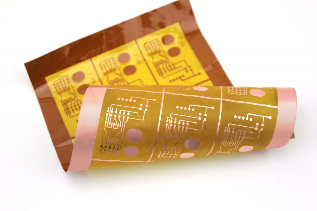
PCB Prototyping is the way to speed up development cycles in electronics design. Laser structuring of copper clad PCB substrate materials directly from the CAD data provides fast realization and fast proof of your electronic circuit.
Thanks to the chemical-free S&S process precise and clean prototypes are possible in minutes without burning the substrate material.
Especially RF and microwave circuits benefit from exact feature dimensions and straight edges, providing a perfect fit of the circuit to the simulation results.
DirectLaser U2 – the Swiss knife for laser micromachining in the lab
DCTs most-sold laser machine for PCB prototyping turns out to be a real universal micromachining tool. Equipped with a UV laser source the DirectLaser U2 processes a wide range of materials such as metal layers, ceramic and organic substrates with micrometer precision in various ways.
Possible processes include:
- Structuring of copper clad PCB substrates with the S&S process
- Cutting and drilling of rigid PCBs
- Drilling of microvias and blind vias on HDI boards
- Cutting and drilling of flexible PCBs
- Kiss-cutting of cover foils
- Decapping of flex-rigid PCBs
- Cutting and structuring of metal foils
- Cutting and drilling of ceramic and green tape materials
- Structuring of metal layers with ceramic substrates
- Structuring of TCO layers on various materials
- Selective removal of coatings and masks
- Depth-controlled selective removal of layers
- Depaneling of populated boards
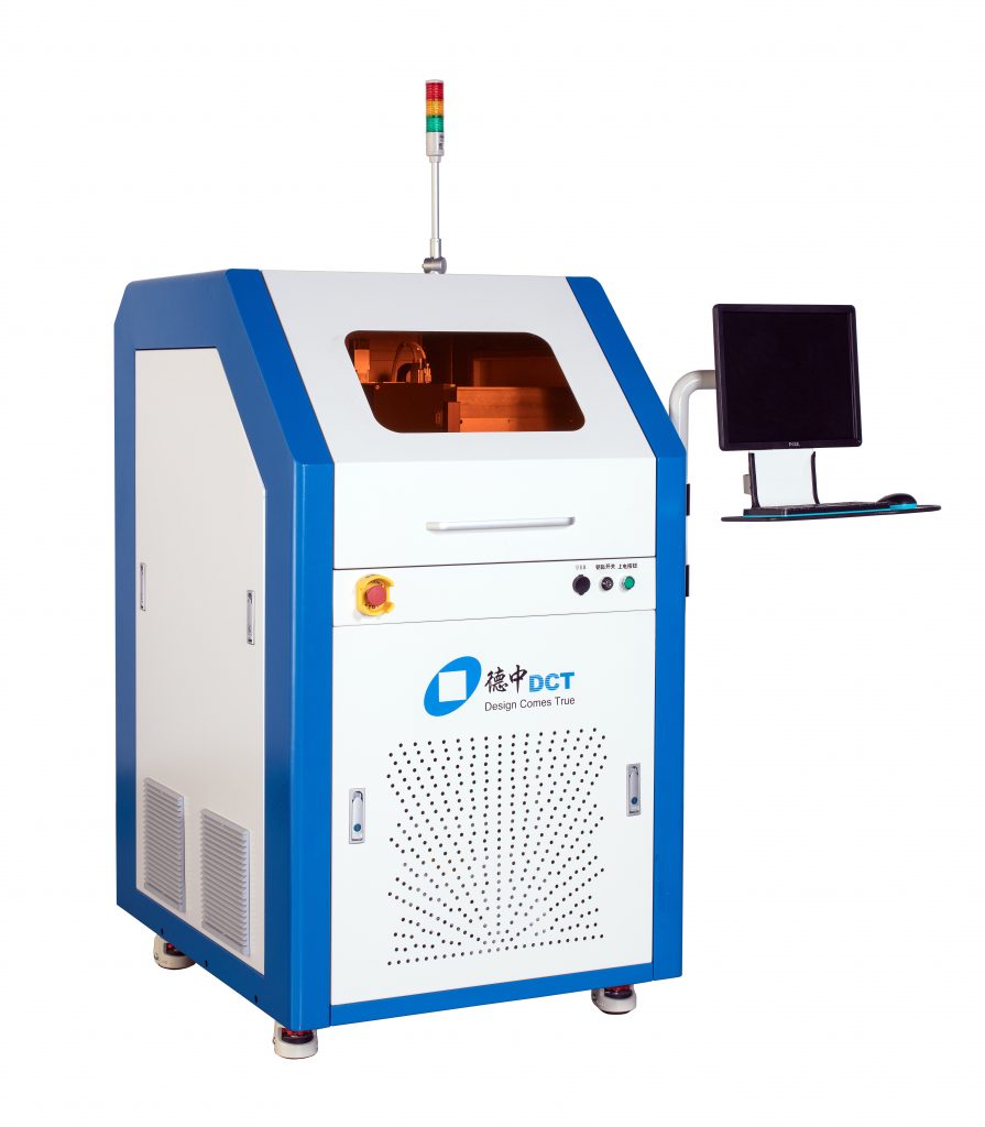
DirectLaser U2 is a compact, but complete laser system designed for laboratory use. Its powerful software package including CirciutCAM 7 and DreamCreaTor guaranties the flexibility needed in a creative lab environment. No surprise we are still learning from our users, what else is possible with the Swiss knife for laser microprocessing.
The DirectLaser U seriescomes with a CE declaration, verified by an international certification body.